 CLOSE SIDEBAR
EL 39 - Logic Gate Identifier with Fault detection
Electronics Projects
Logic gates, like the 74xx series, are commonly used in both education and hobbyist activities. Due to their small nature, the only information on the devices is their product number. Besides memorizing every chip, the only option is to work with the datasheets when using these devices. Our project seeks to alleviate the struggle with the datasheets, as well as assist with troubleshooting. The LGI will inform the user of both the pinout information and the type of logic chip; the most common information one might require. Beyond that, if the chip is faulty, it will display a fault or error signal to the user. So far, the only devices on the market that are similar to this only test transistors, therefore this logic gate identifier will be a new solution to the problem. The logic gate analyzer, as of now, can identify and give the input/output pinout information for AND gates, OR gates, NAND gates, NOR gates, and Inverters or NOT gates.
The previous iteration of this project required the user to know the type of TTL that was being used which meant it was only useful for detecting faults. Furthermore, the previous system stated if each individual gate passed or failed to the user which took up a majority of our available code space, as well as slowing down the testing time. To fix these problems the current version does not make the user enter what type of TTL they are testing, and no longer uses the individual gate result screen. This shortens the code and allows the logic gate identifier to be able to run all TTL units, as well as test a great deal faster due to the more efficient code.
In terms of future advancements of the logic gate identifier, developments are being planned to streamline the LGI even further. The first planned improvement is to make the analysis hold memory of previous gate tests internally which will allow the system to eliminate impossible TTL unit types faster as it tests.
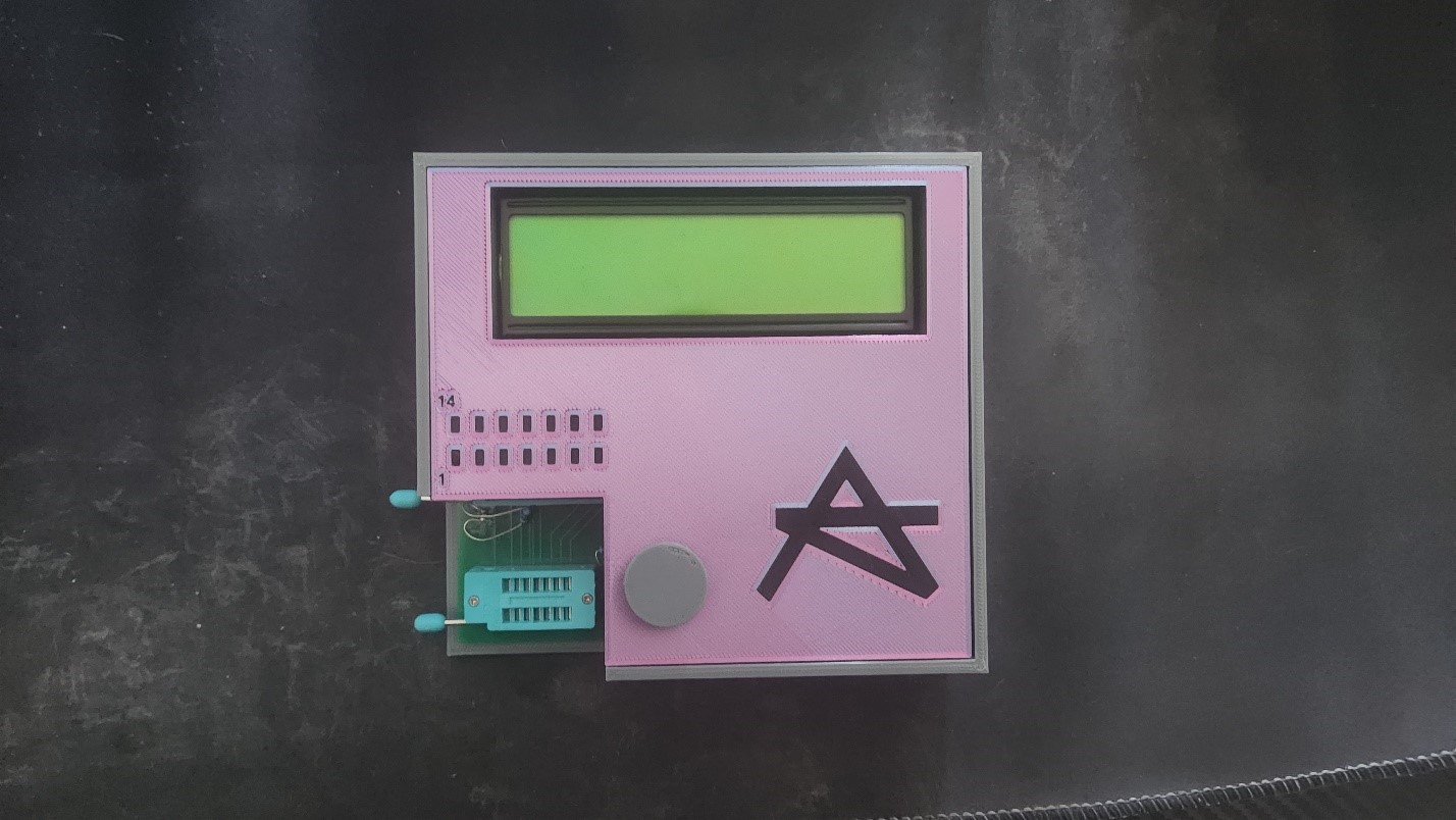
The components of the logic gate identifier were chosen for individual important reasons. The PIC microcontroller was chosen due to its being fiscally reasonable as an investment, as well as its familiar coding language and system. The ZIF IC Socket was chosen to allow the user to input the chip without bending or damaging the legs. The LCD was chosen to allow for a large user interface screen which grants clear visibility. It is also compatible with the previous iteration’s code, to allow for an easy transition to the current interface. The other devices that make up the logic gate identifier such as the battery socket and five-volt regulator were chosen intentionally as well. However, the three main components of this device are the ones that were given the most thought into. All of these components were then measured and graphed onto a PCB board, to then be built and soldered to create the body of the logic gate identifier. A 3D printed casing was then designed to fit the PCB both to supplement the devices task as well as to allow for taking apart to inspect the inner workings of the device.
Updated
2 years ago
Powered by Acadiate
© 2011-2026, Acadiate Inc. or its affiliates · Privacy